ASML - Canon's Nanoimprint Lithography: Finally An ASML Competitor At The 5nm Node
2023-11-01 11:41:34 ET
Summary
- Canon launched its Nanoimprint Lithography semiconductor manufacturing equipment, which has the potential to compete with ASML's EUV technology currently in production at 4nm.
- Canon's first planned semiconductor application is 3D NAND, followed by DRAM, and then logic chips.
- Canon won't face direct competition from ASML's EUV in 3D NAND production, but with DRAMs and Logic.
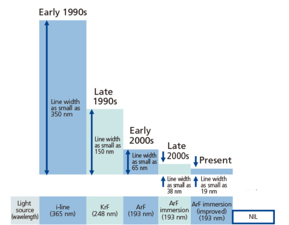
There are three main suppliers of semiconductor lithography equipment: ASML Holding N.V. ( ASML ), Canon Inc. ( CAJPY ), and Nikon Corporation ( OTCPK:NINOY ). ASML is the only supplier of EUV, but also sells i-line, KrF, ArF, and ArF immersion systems (see Chart 1). Canon sells i-line and KrF systems, and Nikon sells i-line, KrF, ArF, and ArF immersion systems.
Chart 1 shows the evolution of optical lithography technology and the linewidth cutoff at which point the user would need to purchase a more advanced system to meet node requirements.
Beyond the optical technology I show NIL. For ASML, this is EUV lithography or Extreme Ultraviolet Lithography. For Canon, this is its "Nanoimprint" lithography, which is the subject of this article based on Canon's new announcement.
Chart 1
For the sub-7nm node, ASML's focus is on EUV insertion, but also sells ArF immersion systems to customers, which could be used with multiple exposure processes to extend DUV lithography below 7nm. Nikon's sub-7nm approach is ArF immersion systems.
Canon is placing its bets on a new and different technology - Nanoimprint Lithography (NIL). Invented at the University of Texas, it was refined by the venture-funded startup Molecular Imprints. Canon acquired Molecular imprints in 2014, and the company was renamed Canon Nanotechnologies, Inc.
According to a press release from the company:
"On October 13, 2023, Canon announced today the launch of the FPA-1200NZ2C nanoimprint semiconductor manufacturing equipment, which executes circuit pattern transfer, the most important semiconductor manufacturing process.
Canon's NIL technology enables patterning with a minimum linewidth of 14 nm, equivalent to the 5nm node required to produce most advanced logic semiconductors which are currently available. With further improvement of mask technology, Canon expects patterning with a minimum linewidth of 10 nm, corresponding to the 2-nm-node."
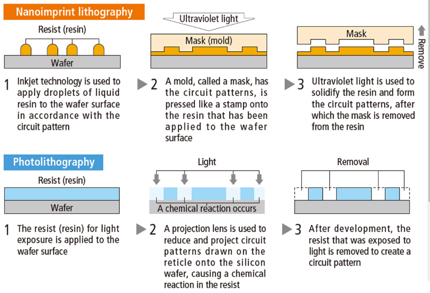
Chart 2 shows the process steps needed with Nanoimprint lithography. Nanoimprint lithography stands apart from conventional lithography by creating nanometer-scale patterns through the direct transfer of a nano-pattern mask (mold) onto a resin-coated wafer surface, entirely devoid of an optical system. This approach ensures precise replication of the intricate circuit patterns from the mask onto the wafer surface, presenting a unique method for high-resolution nanofabrication.
Chart 2
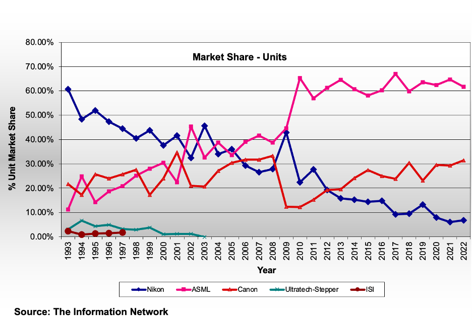
According to The Information Network's report, ASML retained its market leadership in both unit shipments and revenue in 2022. Canon moved into second place since 2013, ahead of Nikon, in unit shipments, as shown in Chart 3.
But there's more to the story than this chart. Different companies led different sectors in 2022:
- Canon led the i-line sector with a 65% share in 2022.
- ASML led the KrF sector with a 70% share.
- ASML led the ArF sector with an 85% share.
- ASML led the ArF immersion sector with an 95% share.
- ASML led the EUV sector with an 100% share.
Thus, Canon, which makes only i-line and KrF systems with a limit of 150nm, according to Chart 1 above, will leapfrog Nikon, which makes ArF immersion systems with a limit of 7nm (when combined with multipatterning) to the 5nm node and be competitive with ASML's EUV technology currently in production at 4nm.
Chart 3
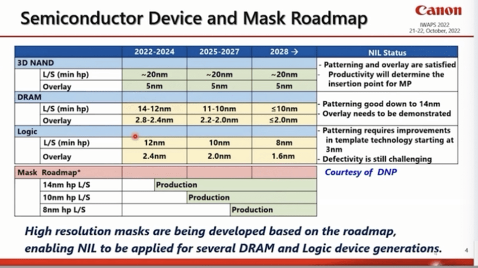
Canon's device roadmap, is shown in Chart 4. The company is first addressing NIL insertion in 3D NAND, primarily at Toshiba Corporation ( OTCPK:TOSYY ) and Western Digital Corporation ( WDC ). DRAM is next, followed by logic. For 3D NAND, NIL has already met requirements for 20nm half-pitch lines and spaces (LS).
Chart 4
Implications from China
ASML has faced restrictions imposed by the Dutch government, preventing the export of its extreme ultraviolet (EUV) lithography machines to China due to the critical role these machines play in the production of the most advanced semiconductor chips. Consequently, ASML has not shipped any of these units to China. This decision is primarily based on concerns about technology transfer and safeguarding sensitive semiconductor manufacturing capabilities.
Canon's recent assertion that its new machine has the potential to enable chip manufacturers to produce semiconductors with a scale as small as 2nm, it is likely that Canon's technology will also face heightened scrutiny and regulatory considerations, as it addresses similar advanced chip manufacturing capabilities that are strategically significant.
Whether or not Canon or other companies can ship non-EUV lithography technology to China, and how it might impact foundries like SMIC (Semiconductor Manufacturing International Corporation) in their chip production capabilities, is subject to various factors and government regulations.
Cost of Ownership
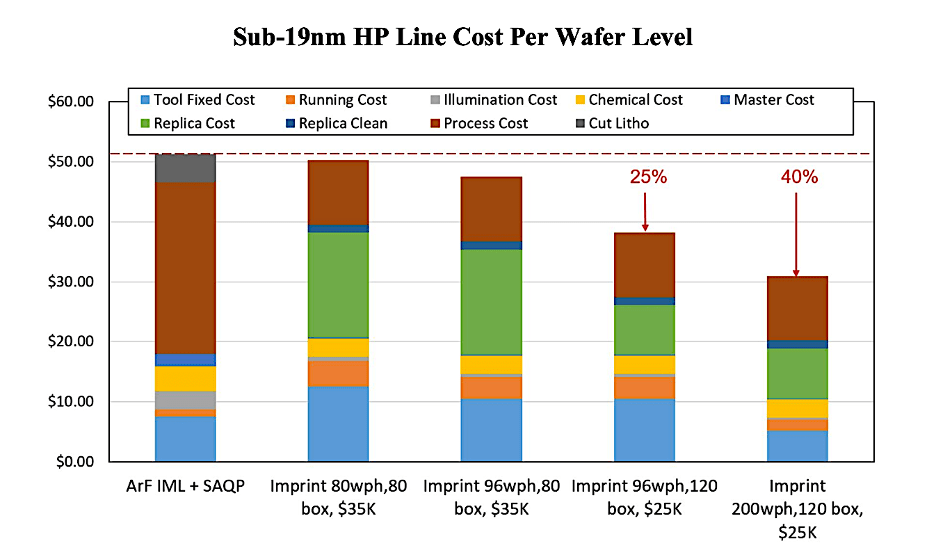
In a direct Nanoimprint Lithography ((NIL)) process, the process involves four key steps: deposition, NIL, etching, and stripping, resulting in a total of eight steps. This process was compared to a conventional ArF immersion process flow for creating dense sub-19nm half pitch lines. In the ArF immersion process, the throughput was assumed to be 275 wafers per hour (wph). An SAQP (Self-Aligned Quadruple Patterning) based process, which included one KrF cut step (typically used for a NAND gate level), necessitated a total of twenty-five steps. The modeling results are illustrated in Chart 5.
Chart 5
The primary factor driving the cost of the ArF immersion process of record ("CoO") is the additional processing steps. Under the conditions described earlier for Nanoimprint Lithography, the cost per wafer level is approximately $2 lower than the ArF immersion process. If the NIL throughput is further increased to 96 wph, the cost advantage over ArF immersion becomes approximately $5 per wafer level.
It's important to highlight that the most significant contributor to the CoO of NIL is the cost of masks. If improvements are made to extend mask life to 120 lots and reduce mask prices to $25,000, the overall mask cost contribution is reduced by about half, resulting in a 25% cost advantage with NIL. Additionally, implementing a multifield imprint process to enhance throughput to 200 wph further reduces the NIL process cost to 40% below the ArF immersion case.
Investor Takeaway
ASML sells EUV systems primarily for Logic (microprocessors) and DRAM memory. Canon's first planned semiconductor application is 3D NAND. The 20nm dimensions on 3D-NAND do not warrant the expense and complexity of an EUV system. Because of this, Canon has a window of opportunity to refine its imprint technology. Memory giants SK hynix and Kioxia Holdings (initially as Toshiba) had been evaluating imprints for nearly 10 years, but faced challenges such as high defect rates that had hindered previous attempts. In fact, Toshiba planned to begin production in fiscal 2017 at a location in Yokkaichi, a city in Mie Prefecture. Evidently that has now been resolved.
Following 3D-NAND, Canon will move to DRAMs. Here it faces direct competition from ASML's EUV, since the company has already sold multiple systems to SK hynix, Samsung Electronics Co., Ltd. ( OTCPK:SSNLF ) and Micron Technology, Inc. ( MU ). The first two companies are already in EUV production, and MU will move to EUV in 2025. Samsung also makes 3D-NAND, the company could move to imprint as the number of layers increases.
While Canon points out that its imprint system is capable of delineating 5nm and 2nm in the future, its internal analysis addresses Cost of Ownership compared to DUV immersion lithography tools, as discussed above. Importantly, it must be remembered and illustrated in Chart 1 above, that immersion lithography's limit is 38nm. To get lower, multiple patterning processes are needed. In the illustration in Chart 5 above, at 19nm, that is 25 additional steps, resulting an imprint CoO advantage of 40% over the ArF immersion case.
I rate Canon a Hold until I start seeing metrics from the system in a production environment.
For further details see:
Canon's Nanoimprint Lithography: Finally An ASML Competitor At The 5nm Node